Download this example
Download this example as a Jupyter Notebook or as a Python script.
Import Stackup#
This example shows how to import stackup file.
Perform imports and define constants#
Perform required imports.
[1]:
import json
import toml
from pathlib import Path
import tempfile

from IPython.display import display
from ansys.aedt.core.examples.downloads import download_file
import pandas as pd
from pyedb import Edb
Define constants.
[2]:
AEDT_VERSION = "2025.1"
NG_MODE = False
Download the example PCB data.
[3]:
temp_folder = tempfile.TemporaryDirectory(suffix=".ansys")
file_edb = download_file(source="edb/ANSYS-HSD_V1.aedb", local_path=temp_folder.name)
Load example layout.#
[4]:
edbapp = Edb(file_edb, edbversion=AEDT_VERSION)
PyAEDT INFO: Star initializing Edb 04:05:02.158872
PyAEDT INFO: Edb version 2025.1
PyAEDT INFO: Logger is initialized in EDB.
PyAEDT INFO: legacy v0.54.0
PyAEDT INFO: Python version 3.10.11 (tags/v3.10.11:7d4cc5a, Apr  5 2023, 00:38:17) [MSC v.1929 64 bit (AMD64)]
PyAEDT INFO: Database ANSYS-HSD_V1.aedb Opened in 2025.1
PyAEDT INFO: Cell main Opened
PyAEDT INFO: Builder was initialized.
PyAEDT INFO: EDB initialized.Time lapse 0:00:10.235295
Review original stackup definition#
Get original stackup definition in a dictionary. Alternatively, stackup definition can be exported in a json file by edbapp.configuration.export()
[5]:
data_cfg = edbapp.configuration.get_data_from_db(stackup=True)
PyAEDT INFO: Getting data from layout database.
[6]:
df = pd.DataFrame(data=data_cfg["stackup"]["layers"])
display(df)
| name | type | material | fill_material | thickness | roughness | etching | |
|---|---|---|---|---|---|---|---|
| 0 | 1_Top | signal | copper | Solder Resist | 0.035mm | {'enabled': False, 'top': {'model': 'huray', '... | {'factor': '0', 'etch_power_ground_nets': Fals... |
| 1 | DE1 | dielectric | Megtron4 | 0.1mm | {'enabled': False, 'top': {'model': 'huray', '... | {'factor': '0', 'etch_power_ground_nets': Fals... | |
| 2 | Inner1(GND1) | signal | copper | Megtron4_2 | 0.017mm | {'enabled': False, 'top': {'model': 'huray', '... | {'factor': '0', 'etch_power_ground_nets': Fals... |
| 3 | DE2 | dielectric | Megtron4_2 | 0.088mm | {'enabled': False, 'top': {'model': 'huray', '... | {'factor': '0', 'etch_power_ground_nets': Fals... | |
| 4 | Inner2(PWR1) | signal | copper | Megtron4_2 | 0.017mm | {'enabled': False, 'top': {'model': 'huray', '... | {'factor': '0', 'etch_power_ground_nets': Fals... |
| 5 | DE3 | dielectric | Megtron4 | 0.1mm | {'enabled': False, 'top': {'model': 'huray', '... | {'factor': '0', 'etch_power_ground_nets': Fals... | |
| 6 | Inner3(Sig1) | signal | copper | Megtron4_3 | 0.017mm | {'enabled': False, 'top': {'model': 'huray', '... | {'factor': '0', 'etch_power_ground_nets': Fals... |
| 7 | Megtron4-1mm | dielectric | Megtron4_3 | 1mm | {'enabled': False, 'top': {'model': 'huray', '... | {'factor': '0', 'etch_power_ground_nets': Fals... | |
| 8 | Inner4(Sig2) | signal | copper | Megtron4_3 | 0.017mm | {'enabled': False, 'top': {'model': 'huray', '... | {'factor': '0', 'etch_power_ground_nets': Fals... |
| 9 | DE5 | dielectric | Megtron4 | 0.1mm | {'enabled': False, 'top': {'model': 'huray', '... | {'factor': '0', 'etch_power_ground_nets': Fals... | |
| 10 | Inner5(PWR2) | signal | copper | Megtron4_2 | 0.017mm | {'enabled': False, 'top': {'model': 'huray', '... | {'factor': '0', 'etch_power_ground_nets': Fals... |
| 11 | DE6 | dielectric | Megtron4_2 | 0.088mm | {'enabled': False, 'top': {'model': 'huray', '... | {'factor': '0', 'etch_power_ground_nets': Fals... | |
| 12 | Inner6(GND2) | signal | copper | Megtron4_2 | 0.017mm | {'enabled': False, 'top': {'model': 'huray', '... | {'factor': '0', 'etch_power_ground_nets': Fals... |
| 13 | DE7 | dielectric | Megtron4 | 0.1mm | {'enabled': False, 'top': {'model': 'huray', '... | {'factor': '0', 'etch_power_ground_nets': Fals... | |
| 14 | 16_Bottom | signal | copper | Solder Resist | 0.035mm | {'enabled': False, 'top': {'model': 'huray', '... | {'factor': '0', 'etch_power_ground_nets': Fals... |
| 15 | Measures | measure | NaN | NaN | NaN | NaN | NaN |
| 16 | SIwave Regions | siwavehfsssolverregions | NaN | NaN | NaN | NaN | NaN |
| 17 | Top Overlay | silkscreen | NaN | NaN | NaN | NaN | NaN |
| 18 | Top Solder | soldermask | NaN | NaN | NaN | NaN | NaN |
| 19 | Bottom Solder | soldermask | NaN | NaN | NaN | NaN | NaN |
| 20 | Bottom Overlay | silkscreen | NaN | NaN | NaN | NaN | NaN |
| 21 | Outline | outline | NaN | NaN | NaN | NaN | NaN |
| 22 | Rats | airlines | NaN | NaN | NaN | NaN | NaN |
| 23 | Errors | errors | NaN | NaN | NaN | NaN | NaN |
| 24 | Symbols | symbol | NaN | NaN | NaN | NaN | NaN |
| 25 | Postprocessing | postprocessing | NaN | NaN | NaN | NaN | NaN |
Modify stackup#
Modify top layer thickness
[7]:
data_cfg["stackup"]["layers"][0]["thickness"] = 0.00005
Add a solder mask layer
[8]:
data_cfg["stackup"]["layers"].insert(
    0, {"name": "soler_mask", "type": "dielectric", "material": "Megtron4", "fill_material": "", "thickness": 0.00002}
)
Review modified stackup
[9]:
df = pd.DataFrame(data=data_cfg["stackup"]["layers"])
display(df.head(3))
| name | type | material | fill_material | thickness | roughness | etching | |
|---|---|---|---|---|---|---|---|
| 0 | soler_mask | dielectric | Megtron4 | 0.00002 | NaN | NaN | |
| 1 | 1_Top | signal | copper | Solder Resist | 0.00005 | {'enabled': False, 'top': {'model': 'huray', '... | {'factor': '0', 'etch_power_ground_nets': Fals... |
| 2 | DE1 | dielectric | Megtron4 | 0.1mm | {'enabled': False, 'top': {'model': 'huray', '... | {'factor': '0', 'etch_power_ground_nets': Fals... |
Write stackup definition into a json file
[10]:
file_cfg = Path(temp_folder.name) / "edb_configuration.json"
with open(file_cfg, "w") as f:
    json.dump(data_cfg, f, indent=4, ensure_ascii=False)
Equivalent toml file looks like below
[11]:
toml_string = toml.dumps(data_cfg)
print(toml_string)
[stackup]
[[stackup.materials]]
conductivity = 58000000.0
dielectric_loss_tangent = 0.0
magnetic_loss_tangent = 0.0
mass_density = 0.0
permittivity = 0.0
permeability = 0.0
poisson_ratio = 0.0
specific_heat = 0.0
thermal_conductivity = 0.0
youngs_modulus = 0.0
thermal_expansion_coefficient = 0.0
name = "copper"

[[stackup.materials]]
conductivity = 0.0
dielectric_loss_tangent = 0.02
magnetic_loss_tangent = 0.0
mass_density = 1900.0
permittivity = 4.4
permeability = 0.0
poisson_ratio = 0.28
specific_heat = 1150.0
thermal_conductivity = 0.294
youngs_modulus = 11000000000.0
thermal_expansion_coefficient = 1.5e-5
name = "FR4_epoxy"

[[stackup.materials]]
conductivity = 0.0
dielectric_loss_tangent = 0.005
magnetic_loss_tangent = 0.0
mass_density = 0.0
permittivity = 3.77
permeability = 0.0
poisson_ratio = 0.0
specific_heat = 0.0
thermal_conductivity = 0.0
youngs_modulus = 0.0
thermal_expansion_coefficient = 0.0
name = "Megtron4"

[[stackup.materials]]
conductivity = 0.0
dielectric_loss_tangent = 0.006
magnetic_loss_tangent = 0.0
mass_density = 0.0
permittivity = 3.47
permeability = 0.0
poisson_ratio = 0.0
specific_heat = 0.0
thermal_conductivity = 0.0
youngs_modulus = 0.0
thermal_expansion_coefficient = 0.0
name = "Megtron4_2"

[[stackup.materials]]
conductivity = 0.0
dielectric_loss_tangent = 0.005
magnetic_loss_tangent = 0.0
mass_density = 0.0
permittivity = 4.2
permeability = 0.0
poisson_ratio = 0.0
specific_heat = 0.0
thermal_conductivity = 0.0
youngs_modulus = 0.0
thermal_expansion_coefficient = 0.0
name = "Megtron4_3"

[[stackup.materials]]
conductivity = 0.0
dielectric_loss_tangent = 0.0
magnetic_loss_tangent = 0.0
mass_density = 0.0
permittivity = 3.0
permeability = 0.0
poisson_ratio = 0.0
specific_heat = 0.0
thermal_conductivity = 0.0
youngs_modulus = 0.0
thermal_expansion_coefficient = 0.0
name = "Solder Resist"

[[stackup.layers]]
name = "soler_mask"
type = "dielectric"
material = "Megtron4"
fill_material = ""
thickness = 2e-5

[[stackup.layers]]
name = "1_Top"
type = "signal"
material = "copper"
fill_material = "Solder Resist"
thickness = 5e-5

[stackup.layers.roughness]
enabled = false
[stackup.layers.etching]
factor = "0"
etch_power_ground_nets = false
enabled = false
[stackup.layers.roughness.top]
model = "huray"
nodule_radius = "0"
surface_ratio = "0"
[stackup.layers.roughness.bottom]
model = "huray"
nodule_radius = "0"
surface_ratio = "0"
[stackup.layers.roughness.side]
model = "huray"
nodule_radius = "0"
surface_ratio = "0"
[[stackup.layers]]
name = "DE1"
type = "dielectric"
material = "Megtron4"
fill_material = ""
thickness = "0.1mm"

[stackup.layers.roughness]
enabled = false
[stackup.layers.etching]
factor = "0"
etch_power_ground_nets = false
enabled = false
[stackup.layers.roughness.top]
model = "huray"
nodule_radius = "0"
surface_ratio = "0"
[stackup.layers.roughness.bottom]
model = "huray"
nodule_radius = "0"
surface_ratio = "0"
[stackup.layers.roughness.side]
model = "huray"
nodule_radius = "0"
surface_ratio = "0"
[[stackup.layers]]
name = "Inner1(GND1)"
type = "signal"
material = "copper"
fill_material = "Megtron4_2"
thickness = "0.017mm"

[stackup.layers.roughness]
enabled = false
[stackup.layers.etching]
factor = "0"
etch_power_ground_nets = false
enabled = false
[stackup.layers.roughness.top]
model = "huray"
nodule_radius = "0"
surface_ratio = "0"
[stackup.layers.roughness.bottom]
model = "huray"
nodule_radius = "0"
surface_ratio = "0"
[stackup.layers.roughness.side]
model = "huray"
nodule_radius = "0"
surface_ratio = "0"
[[stackup.layers]]
name = "DE2"
type = "dielectric"
material = "Megtron4_2"
fill_material = ""
thickness = "0.088mm"

[stackup.layers.roughness]
enabled = false
[stackup.layers.etching]
factor = "0"
etch_power_ground_nets = false
enabled = false
[stackup.layers.roughness.top]
model = "huray"
nodule_radius = "0"
surface_ratio = "0"
[stackup.layers.roughness.bottom]
model = "huray"
nodule_radius = "0"
surface_ratio = "0"
[stackup.layers.roughness.side]
model = "huray"
nodule_radius = "0"
surface_ratio = "0"
[[stackup.layers]]
name = "Inner2(PWR1)"
type = "signal"
material = "copper"
fill_material = "Megtron4_2"
thickness = "0.017mm"

[stackup.layers.roughness]
enabled = false
[stackup.layers.etching]
factor = "0"
etch_power_ground_nets = false
enabled = false
[stackup.layers.roughness.top]
model = "huray"
nodule_radius = "0"
surface_ratio = "0"
[stackup.layers.roughness.bottom]
model = "huray"
nodule_radius = "0"
surface_ratio = "0"
[stackup.layers.roughness.side]
model = "huray"
nodule_radius = "0"
surface_ratio = "0"
[[stackup.layers]]
name = "DE3"
type = "dielectric"
material = "Megtron4"
fill_material = ""
thickness = "0.1mm"

[stackup.layers.roughness]
enabled = false
[stackup.layers.etching]
factor = "0"
etch_power_ground_nets = false
enabled = false
[stackup.layers.roughness.top]
model = "huray"
nodule_radius = "0"
surface_ratio = "0"
[stackup.layers.roughness.bottom]
model = "huray"
nodule_radius = "0"
surface_ratio = "0"
[stackup.layers.roughness.side]
model = "huray"
nodule_radius = "0"
surface_ratio = "0"
[[stackup.layers]]
name = "Inner3(Sig1)"
type = "signal"
material = "copper"
fill_material = "Megtron4_3"
thickness = "0.017mm"

[stackup.layers.roughness]
enabled = false
[stackup.layers.etching]
factor = "0"
etch_power_ground_nets = false
enabled = false
[stackup.layers.roughness.top]
model = "huray"
nodule_radius = "0"
surface_ratio = "0"
[stackup.layers.roughness.bottom]
model = "huray"
nodule_radius = "0"
surface_ratio = "0"
[stackup.layers.roughness.side]
model = "huray"
nodule_radius = "0"
surface_ratio = "0"
[[stackup.layers]]
name = "Megtron4-1mm"
type = "dielectric"
material = "Megtron4_3"
fill_material = ""
thickness = "1mm"

[stackup.layers.roughness]
enabled = false
[stackup.layers.etching]
factor = "0"
etch_power_ground_nets = false
enabled = false
[stackup.layers.roughness.top]
model = "huray"
nodule_radius = "0"
surface_ratio = "0"
[stackup.layers.roughness.bottom]
model = "huray"
nodule_radius = "0"
surface_ratio = "0"
[stackup.layers.roughness.side]
model = "huray"
nodule_radius = "0"
surface_ratio = "0"
[[stackup.layers]]
name = "Inner4(Sig2)"
type = "signal"
material = "copper"
fill_material = "Megtron4_3"
thickness = "0.017mm"

[stackup.layers.roughness]
enabled = false
[stackup.layers.etching]
factor = "0"
etch_power_ground_nets = false
enabled = false
[stackup.layers.roughness.top]
model = "huray"
nodule_radius = "0"
surface_ratio = "0"
[stackup.layers.roughness.bottom]
model = "huray"
nodule_radius = "0"
surface_ratio = "0"
[stackup.layers.roughness.side]
model = "huray"
nodule_radius = "0"
surface_ratio = "0"
[[stackup.layers]]
name = "DE5"
type = "dielectric"
material = "Megtron4"
fill_material = ""
thickness = "0.1mm"

[stackup.layers.roughness]
enabled = false
[stackup.layers.etching]
factor = "0"
etch_power_ground_nets = false
enabled = false
[stackup.layers.roughness.top]
model = "huray"
nodule_radius = "0"
surface_ratio = "0"
[stackup.layers.roughness.bottom]
model = "huray"
nodule_radius = "0"
surface_ratio = "0"
[stackup.layers.roughness.side]
model = "huray"
nodule_radius = "0"
surface_ratio = "0"
[[stackup.layers]]
name = "Inner5(PWR2)"
type = "signal"
material = "copper"
fill_material = "Megtron4_2"
thickness = "0.017mm"

[stackup.layers.roughness]
enabled = false
[stackup.layers.etching]
factor = "0"
etch_power_ground_nets = false
enabled = false
[stackup.layers.roughness.top]
model = "huray"
nodule_radius = "0"
surface_ratio = "0"
[stackup.layers.roughness.bottom]
model = "huray"
nodule_radius = "0"
surface_ratio = "0"
[stackup.layers.roughness.side]
model = "huray"
nodule_radius = "0"
surface_ratio = "0"
[[stackup.layers]]
name = "DE6"
type = "dielectric"
material = "Megtron4_2"
fill_material = ""
thickness = "0.088mm"

[stackup.layers.roughness]
enabled = false
[stackup.layers.etching]
factor = "0"
etch_power_ground_nets = false
enabled = false
[stackup.layers.roughness.top]
model = "huray"
nodule_radius = "0"
surface_ratio = "0"
[stackup.layers.roughness.bottom]
model = "huray"
nodule_radius = "0"
surface_ratio = "0"
[stackup.layers.roughness.side]
model = "huray"
nodule_radius = "0"
surface_ratio = "0"
[[stackup.layers]]
name = "Inner6(GND2)"
type = "signal"
material = "copper"
fill_material = "Megtron4_2"
thickness = "0.017mm"

[stackup.layers.roughness]
enabled = false
[stackup.layers.etching]
factor = "0"
etch_power_ground_nets = false
enabled = false
[stackup.layers.roughness.top]
model = "huray"
nodule_radius = "0"
surface_ratio = "0"
[stackup.layers.roughness.bottom]
model = "huray"
nodule_radius = "0"
surface_ratio = "0"
[stackup.layers.roughness.side]
model = "huray"
nodule_radius = "0"
surface_ratio = "0"
[[stackup.layers]]
name = "DE7"
type = "dielectric"
material = "Megtron4"
fill_material = ""
thickness = "0.1mm"

[stackup.layers.roughness]
enabled = false
[stackup.layers.etching]
factor = "0"
etch_power_ground_nets = false
enabled = false
[stackup.layers.roughness.top]
model = "huray"
nodule_radius = "0"
surface_ratio = "0"
[stackup.layers.roughness.bottom]
model = "huray"
nodule_radius = "0"
surface_ratio = "0"
[stackup.layers.roughness.side]
model = "huray"
nodule_radius = "0"
surface_ratio = "0"
[[stackup.layers]]
name = "16_Bottom"
type = "signal"
material = "copper"
fill_material = "Solder Resist"
thickness = "0.035mm"

[stackup.layers.roughness]
enabled = false
[stackup.layers.etching]
factor = "0"
etch_power_ground_nets = false
enabled = false
[stackup.layers.roughness.top]
model = "huray"
nodule_radius = "0"
surface_ratio = "0"
[stackup.layers.roughness.bottom]
model = "huray"
nodule_radius = "0"
surface_ratio = "0"
[stackup.layers.roughness.side]
model = "huray"
nodule_radius = "0"
surface_ratio = "0"
[[stackup.layers]]
name = "Measures"
type = "measure"

[[stackup.layers]]
name = "SIwave Regions"
type = "siwavehfsssolverregions"

[[stackup.layers]]
name = "Top Overlay"
type = "silkscreen"

[[stackup.layers]]
name = "Top Solder"
type = "soldermask"

[[stackup.layers]]
name = "Bottom Solder"
type = "soldermask"

[[stackup.layers]]
name = "Bottom Overlay"
type = "silkscreen"

[[stackup.layers]]
name = "Outline"
type = "outline"

[[stackup.layers]]
name = "Rats"
type = "airlines"

[[stackup.layers]]
name = "Errors"
type = "errors"

[[stackup.layers]]
name = "Symbols"
type = "symbol"

[[stackup.layers]]
name = "Postprocessing"
type = "postprocessing"
Load stackup from json configuration file#
[12]:
edbapp.configuration.load(file_cfg, apply_file=True)
PyAEDT INFO: Updating boundaries finished. Time lapse 0:00:00.015568
PyAEDT INFO: Updating nets finished. Time lapse 0:00:00
PyAEDT INFO: Updating components finished. Time lapse 0:00:00
PyAEDT INFO: Creating pin groups finished. Time lapse 0:00:00
PyAEDT INFO: Placing sources finished. Time lapse 0:00:00
PyAEDT INFO: Creating setups finished. Time lapse 0:00:00
PyAEDT INFO: Applying materials finished. Time lapse 0:00:00.015631
PyAEDT INFO: Updating stackup finished. Time lapse 0:00:11.469521
PyAEDT INFO: Applying padstacks finished. Time lapse 0:00:00
PyAEDT INFO: Applying S-parameters finished. Time lapse 0:00:00
PyAEDT INFO: Applying package definitions finished. Time lapse 0:00:00
PyAEDT INFO: Applying modeler finished. Time lapse 0:00:00.531296
PyAEDT INFO: Placing ports finished. Time lapse 0:00:00
PyAEDT INFO: Placing probes finished. Time lapse 0:00:00
PyAEDT INFO: Applying operations finished. Time lapse 0:00:00
[12]:
<pyedb.configuration.cfg_data.CfgData at 0x19c19e33dc0>
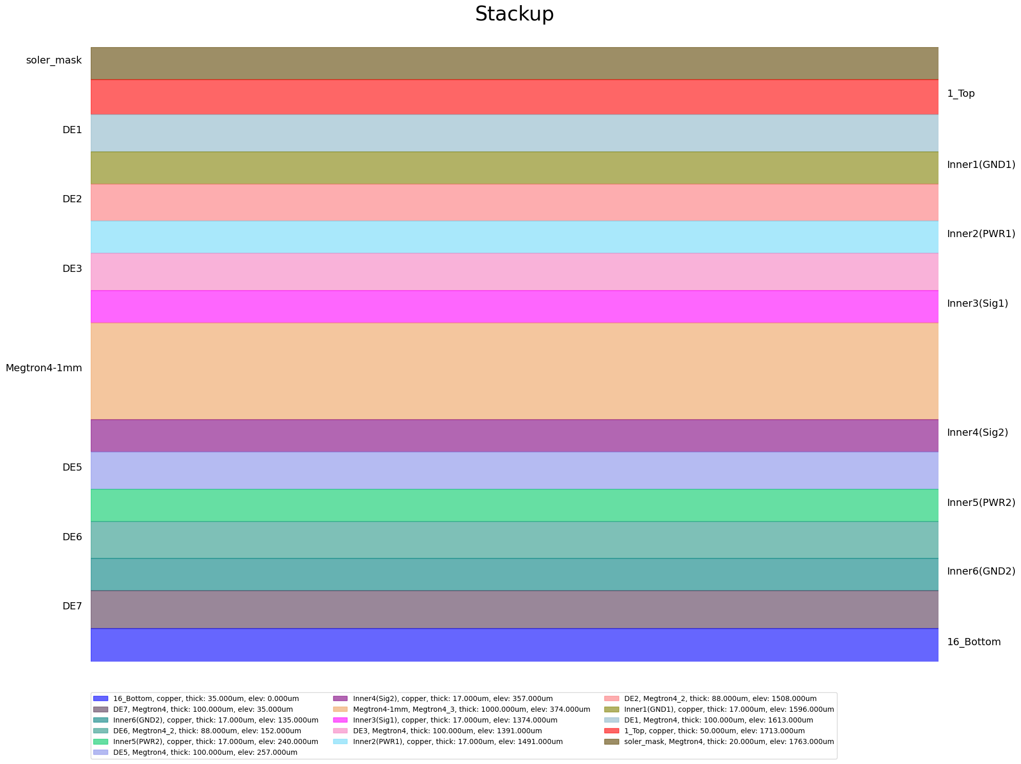
Plot stackup
[13]:
edbapp.stackup.plot()
[13]:
<module 'matplotlib.pyplot' from 'C:\\actions-runner\\_work\\pyaedt-examples\\pyaedt-examples\\.venv\\lib\\site-packages\\matplotlib\\pyplot.py'>
Check top layer thickness
[14]:
edbapp.stackup["1_Top"].thickness
[14]:
5e-05
Save and close Edb#
The temporary folder will be deleted once the execution of this script is finished. Replace edbapp.save() with edbapp.save_as(“C:/example.aedb”) to keep the example project.
[15]:
edbapp.save()
edbapp.close()
PyAEDT INFO: EDB file save time: 0.00ms
PyAEDT INFO: EDB file release time: 0.00ms
[15]:
True
Download this example
Download this example as a Jupyter Notebook or as a Python script.