Download this example
Download this example as a Jupyter Notebook or as a Python script.
Pre-layout signal integrity#
This example shows how to create a parameterized layout design and load the layout into HFSS 3D Layout for analysis and postprocessing.
Create EDB:
Add material.
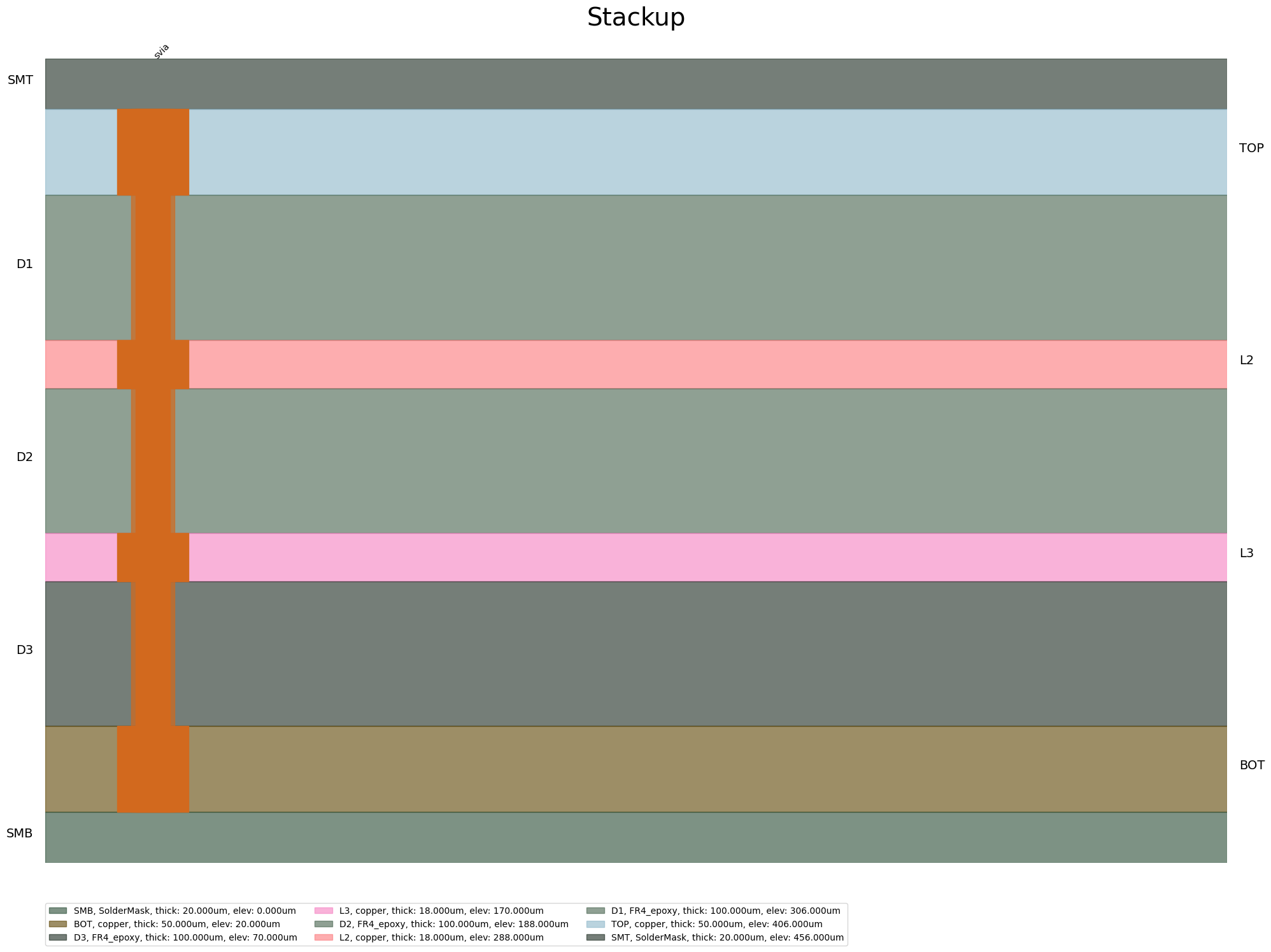
Create stackup.
Create a parameterized via padstack definition.
Create ground planes.
Create a component.
Create signal vias and traces.
Create ground stitching vias.
Create HFSS analysis setup and frequency sweep.
Import EDB into HFSS 3D Layout:
Place SMA connector.
Analyze.
Plot return loss.
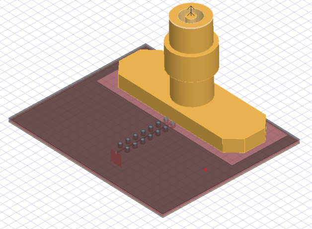
Here is an image of the model that is created in this example.

Keywords: HFSS 3D Layout, signal integrity.
Perform imports and define constants#
Perform required packages.
[1]:
import os
import tempfile
import time

from ansys.aedt.core import Hfss3dLayout
from ansys.aedt.core.examples.downloads import download_file
from pyedb import Edb
Define constants.
[2]:
AEDT_VERSION = "2025.2"
NUM_CORES = 4
NG_MODE = False  # Open AEDT UI when it is launched.
Create temporary directory and download example files#
Create a temporary directory where downloaded data or dumped data can be stored. If you’d like to retrieve the project data for subsequent use, the temporary folder name is given by temp_folder.name.
[3]:
temp_folder = tempfile.TemporaryDirectory(suffix=".ansys")
sma_rf_connector = download_file(
    source="component_3d",
    name="SMA_RF_SURFACE_MOUNT.a3dcomp",
    local_path=temp_folder.name,
)
Create layout design#
Import example design#
[4]:
aedb = os.path.join(temp_folder.name, "new_layout.aedb")
edbapp = Edb(edbpath=aedb, version=AEDT_VERSION)
PyEDB INFO: Star initializing Edb 07:12:54.797195
PyEDB INFO: Edb version 2025.2
PyEDB INFO: Logger is initialized. Log file is saved to C:\Users\ansys\AppData\Local\Temp\pyedb_ansys.log.
PyEDB INFO: legacy v0.71.0
PyEDB INFO: Python version 3.10.11 (tags/v3.10.11:7d4cc5a, Apr  5 2023, 00:38:17) [MSC v.1929 64 bit (AMD64)]
PyEDB INFO: create_edb completed in 9.1181 seconds.
PyEDB INFO: EDB C:\Users\ansys\AppData\Local\Temp\tmps6n94ocx.ansys\new_layout.aedb created correctly.
PyEDB INFO: EDB initialization completed in 9.2274 seconds.
[5]:
# Set antipad always on.
edbapp.design_options.antipads_always_on = True
Add material definitions#
[6]:
edbapp.materials.add_conductor_material(name="copper", conductivity=58000000)
edbapp.materials.add_dielectric_material(name="FR4_epoxy", permittivity=4, dielectric_loss_tangent=0.02)
edbapp.materials.add_dielectric_material(name="solder_mask", permittivity=3.1, dielectric_loss_tangent=0.035)
[6]:
<pyedb.dotnet.database.definition.definition_obj.MaterialDef at 0x1a5a9329510>
Create stackup#
[7]:
edbapp.stackup.create_symmetric_stackup(
    layer_count=4,
    inner_layer_thickness="18um",
    outer_layer_thickness="50um",
    dielectric_thickness="100um",
    dielectric_material="FR4_epoxy",
    soldermask=True,
    soldermask_thickness="20um",
)
[7]:
True
Create parameterized padstack definition#
Create signal via padstack definition.
[8]:
edbapp["$antipad"] = "0.7mm"
edbapp.padstacks.create(padstackname="svia", holediam="0.3mm", antipaddiam="$antipad", paddiam="0.5mm")
PyEDB INFO: Padstack svia create correctly
[8]:
'svia'
Create component pin padstack definition.
[9]:
edbapp.padstacks.create(
    padstackname="comp_pin",
    paddiam="400um",
    antipaddiam="600um",
    start_layer="TOP",
    stop_layer="TOP",
    antipad_shape="Circle",
    has_hole=False,
)
PyEDB INFO: Padstack comp_pin create correctly
[9]:
'comp_pin'
Review stackup#
[10]:
edbapp.stackup.plot(plot_definitions="svia")

[10]:
<module 'matplotlib.pyplot' from 'C:\\actions-runner\\_work\\pyaedt-examples\\pyaedt-examples\\.venv\\lib\\site-packages\\matplotlib\\pyplot.py'>
Create ground planes#
[11]:
board_width = "22mm"
board_length = "18mm"
board_center_point = [0, "5mm"]

gnd_l2 = edbapp.modeler.create_rectangle(
    layer_name="L2",
    net_name="GND",
    center_point=board_center_point,
    width=board_width,
    height=board_length,
    representation_type="CenterWidthHeight",
    corner_radius="0mm",
    rotation="0deg",
)

gnd_l3 = edbapp.modeler.create_rectangle(
    layer_name="L3",
    net_name="GND",
    center_point=board_center_point,
    width=board_width,
    height=board_length,
    representation_type="CenterWidthHeight",
    corner_radius="0mm",
    rotation="0deg",
)

gnd_bottom = edbapp.modeler.create_rectangle(
    layer_name="BOT",
    net_name="GND",
    center_point=board_center_point,
    width=board_width,
    height=board_length,
    representation_type="CenterWidthHeight",
    corner_radius="0mm",
    rotation="0deg",
)
Create a component#
[12]:
edbapp.padstacks.place(
    position=[0, 0],
    definition_name="comp_pin",
    net_name="SIG",
    is_pin=True,
    via_name="1",
)
[12]:
<pyedb.dotnet.database.edb_data.padstacks_data.EDBPadstackInstance at 0x1a5884e6bf0>
[13]:
comp_pins = [
    edbapp.padstacks.place(
        position=["-6mm", 0],
        definition_name="comp_pin",
        net_name="GND",
        is_pin=True,
        via_name="2",
    ),
    edbapp.padstacks.place(
        position=["6mm", 0],
        definition_name="comp_pin",
        net_name="GND",
        is_pin=True,
        via_name="3",
    ),
]
[14]:
comp_u1 = edbapp.components.create(
    pins=comp_pins,
    component_name="U1",
    component_part_name="BGA",
    placement_layer="TOP",
)
comp_u1.create_clearance_on_component(extra_soldermask_clearance=3.5e-3)
PyEDB INFO: Correctly computed Extension at first iteration.
[14]:
True
Place vias#
Place a signal via.
[15]:
edbapp.padstacks.place(position=[0, 0], definition_name="svia", net_name="SIG", is_pin=False)
[15]:
<pyedb.dotnet.database.edb_data.padstacks_data.EDBPadstackInstance at 0x1a58a6666b0>
Place ground stitching vias.
[16]:
edbapp.padstacks.place(position=["-1mm", 0], definition_name="svia", net_name="GND", is_pin=False)
edbapp.padstacks.place(position=["1mm", 0], definition_name="svia", net_name="GND", is_pin=False)
edbapp.padstacks.place(position=[0, "-1mm"], definition_name="svia", net_name="GND", is_pin=False)
edbapp.padstacks.place(position=[0, "1mm"], definition_name="svia", net_name="GND", is_pin=False)
[16]:
<pyedb.dotnet.database.edb_data.padstacks_data.EDBPadstackInstance at 0x1a58a667760>
Create signal traces#
[17]:
edbapp["width"] = "0.15mm"
edbapp["gap"] = "0.1mm"
Create signal fanout.
[18]:
sig_trace = edbapp.modeler.create_trace(
    path_list=[[0, 0]],
    layer_name="BOT",
    width="width",
    net_name="SIG",
    start_cap_style="Round",
    end_cap_style="Round",
    corner_style="Round",
)
[19]:
sig_trace.add_point(x="0.5mm", y="0.5mm", incremental=True)
sig_trace.add_point(x=0, y="1mm", incremental=True)
sig_trace.add_point(x="-0.5mm", y="0.5mm", incremental=True)
sig_trace.add_point(x=0, y="1mm", incremental=True)
sig_path = sig_trace.get_center_line()
Create coplanar waveguide with ground stitching vias.
[20]:
sig2_trace = edbapp.modeler.create_trace(
    path_list=[sig_path[-1]],
    layer_name="BOT",
    width="width",
    net_name="SIG",
    start_cap_style="Round",
    end_cap_style="Flat",
    corner_style="Round",
)
sig2_trace.add_point(x=0, y="6mm", incremental=True)
sig2_trace.create_via_fence(distance="0.5mm", gap="1mm", padstack_name="svia")
sig2_trace.add_point(x=0, y="1mm", incremental=True)
[20]:
True
Create trace-to-ground clearance.
[21]:
sig2_path = sig2_trace.get_center_line()
path_list = [sig_path, sig2_path]
for i in path_list:
    void = edbapp.modeler.create_trace(
        path_list=i,
        layer_name="BOT",
        width="width+gap*2",
        start_cap_style="Round",
        end_cap_style="Round",
        corner_style="Round",
    )
    edbapp.modeler.add_void(shape=gnd_bottom, void_shape=void)
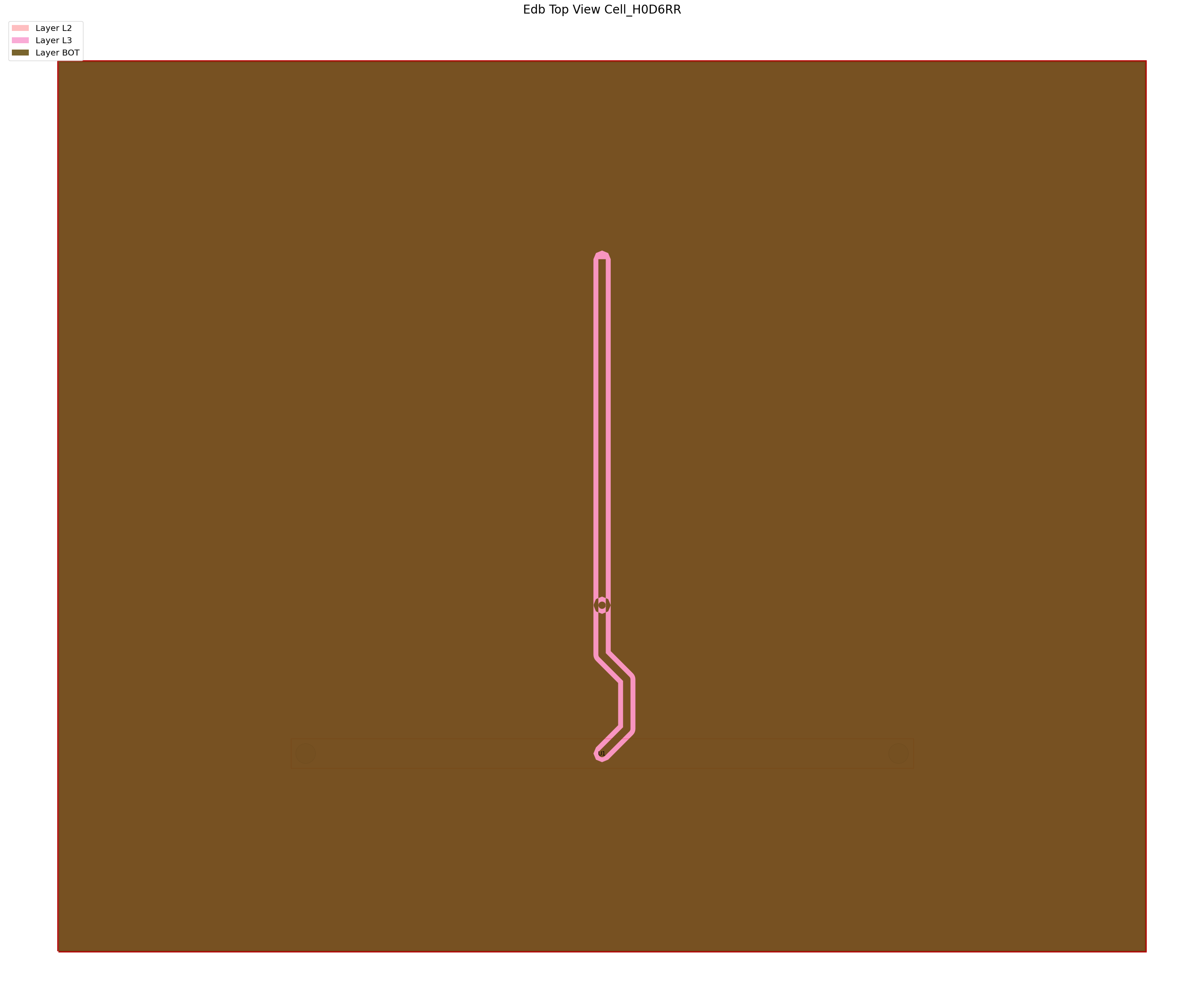
Generate plot to review.
[22]:
edbapp.nets.plot()

PyEDB INFO: Plot Generation time 0.726
[22]:
(<Figure size 6000x3000 with 1 Axes>,
 <Axes: title={'center': 'Edb Top View Cell_N9UWQ7'}>)
Create ports#
Create a wave port.
[23]:
sig2_trace.create_edge_port(
    name="p1_wave_port",
    position="End",
    port_type="Wave",
    reference_layer=None,
    horizontal_extent_factor=10,
    vertical_extent_factor=10,
    pec_launch_width="0.01mm",
)
[23]:
('p1_wave_port',
 <pyedb.dotnet.database.edb_data.ports.WavePort at 0x1a58a6bbb80>)
Create HFSS analysis setup#
[24]:
setup = edbapp.create_hfss_setup("Setup1")
setup.set_solution_single_frequency("5GHz", max_num_passes=1, max_delta_s="0.02")
setup.hfss_solver_settings.order_basis = "first"
C:\Users\ansys\AppData\Local\Temp\ipykernel_7616\797050568.py:1: DeprecationWarning: Call to deprecated function create_hfss_setup. use simulation_setups.create_hfss_setup instead
  setup = edbapp.create_hfss_setup("Setup1")
Add a frequency sweep to the setup.
When the simulation results are to be used for transient SPICE analysis, you should use the following strategy:
DC point
Logarithmic sweep from 1 kHz to 100 MHz
Linear scale for higher frequencies
[25]:
setup.add_frequency_sweep(
    "Sweep1",
    frequency_sweep=[
        ["log scale", "10MHz", "100MHz", 3],
        ["linear scale", "0.1GHz", "5GHz", "0.2GHz"],
    ],
)
[25]:
<pyedb.dotnet.database.sim_setup_data.data.sweep_data.SweepData at 0x1a58a6bb3a0>
Save and close EDB#
[26]:
edbapp.save()
edbapp.close()
PyEDB INFO: Save Edb file completed in 0.0000 seconds.
PyEDB INFO: Close Edb file completed in 0.0345 seconds.
[26]:
True
Analyze in HFSS 3D Layout#
Load EDB into HFSS 3D Layout.#
[27]:
h3d = Hfss3dLayout(aedb, version=AEDT_VERSION, non_graphical=NG_MODE, new_desktop=True)
PyAEDT INFO: Python version 3.10.11 (tags/v3.10.11:7d4cc5a, Apr  5 2023, 00:38:17) [MSC v.1929 64 bit (AMD64)].
PyAEDT INFO: PyAEDT version 1.0.dev0.
PyAEDT INFO: Initializing new Desktop session.
PyAEDT INFO: AEDT version 2025.2.
PyAEDT INFO: New AEDT session is starting on gRPC port 62604.
PyAEDT INFO: Starting new AEDT gRPC session on port 62604.
PyAEDT INFO: Launching AEDT server with gRPC transport mode: wnua
PyAEDT INFO: Electronics Desktop started on gRPC port 62604 after 11.0 seconds.
PyAEDT INFO: AEDT installation Path C:\Program Files\ANSYS Inc\v252\AnsysEM
PyAEDT INFO: Connected to AEDT gRPC session on port 62604.
PyAEDT WARNING: Service Pack is not detected. PyAEDT is currently connecting in Insecure Mode.
PyAEDT WARNING: Please download and install latest Service Pack to use connect to AEDT in Secure Mode.
PyAEDT INFO: EDB folder C:\Users\ansys\AppData\Local\Temp\tmps6n94ocx.ansys\new_layout.aedb has been imported to project new_layout
PyAEDT INFO: Active Design set to 0;Cell_N9UWQ7
PyAEDT INFO: AEDT objects correctly read
Place SMA RF connector#
[28]:
comp = h3d.modeler.place_3d_component(
    component_path=sma_rf_connector,
    number_of_terminals=1,
    placement_layer="TOP",
    component_name="sma_rf",
    pos_x=0,
    pos_y=0,
    create_ports=True,
)
comp.angle = "90deg"
PyAEDT INFO: Loading Modeler.
PyAEDT INFO: Modeler loaded.
PyAEDT INFO: Modeler class has been initialized! Elapsed time: 0m 0sec
Run simulation#
[29]:
h3d.analyze(cores=4)
PyAEDT INFO: Project new_layout Saved correctly
PyAEDT INFO: Key Desktop/ActiveDSOConfigurations/HFSS 3D Layout Design correctly changed.
PyAEDT INFO: Solving all design setups. Analysis started...
PyAEDT INFO: Design setup None solved correctly in 0.0h 1.0m 32.0s
PyAEDT INFO: Key Desktop/ActiveDSOConfigurations/HFSS 3D Layout Design correctly changed.
[29]:
True
Visualize the return loss.#
[30]:
h3d.post.create_report("dB(S(port_1, port_1))")
PyAEDT INFO: Parsing C:\Users\ansys\AppData\Local\Temp\tmps6n94ocx.ansys\new_layout.aedt.
PyAEDT INFO: File C:\Users\ansys\AppData\Local\Temp\tmps6n94ocx.ansys\new_layout.aedt correctly loaded. Elapsed time: 0m 0sec
PyAEDT INFO: aedt file load time 0.03863048553466797
PyAEDT INFO: PostProcessor class has been initialized! Elapsed time: 0m 0sec
PyAEDT INFO: Post class has been initialized! Elapsed time: 0m 0sec
PyAEDT INFO: No EDB gRPC setting provided. Disabling gRPC for EDB.
PyAEDT INFO: Loading EDB with Dotnet enabled.
PyEDB INFO: Star initializing Edb 07:15:21.173142
PyEDB INFO: Edb version 2025.2
PyEDB INFO: Logger is initialized. Log file is saved to C:\Users\ansys\AppData\Local\Temp\pyedb_ansys.log.
PyEDB INFO: legacy v0.71.0
PyEDB INFO: Python version 3.10.11 (tags/v3.10.11:7d4cc5a, Apr  5 2023, 00:38:17) [MSC v.1929 64 bit (AMD64)]
PyEDB INFO: Database new_layout.aedb Opened in 2025.2
PyEDB INFO: Cell Cell_N9UWQ7 Opened
PyEDB INFO: Builder was initialized.
PyEDB INFO: open_edb completed in 0.0388 seconds.
PyEDB INFO: EDB initialization completed in 0.0388 seconds.
PyAEDT ERROR: Failed to create traces on the report. Check input parameters
[30]:
False
Create Field Plot on clip plane#
[31]:
# solutions = h3d.get_touchstone_data()[0]
# solutions.log_x = False
# solutions.plot()
cp_name = h3d.modeler.clip_plane()
[32]:
plot = h3d.post.create_fieldplot_cutplane(cp_name, "Mag_E", h3d.nominal_adaptive, intrinsics={"Freq": "5GHz", "Phase": "0deg"})
PyAEDT INFO: Active Design set to 0;Cell_N9UWQ7
Release AEDT#
[33]:
h3d.save_project()
h3d.release_desktop()
# Wait 3 seconds to allow AEDT to shut down before cleaning the temporary directory.
time.sleep(3)
PyAEDT INFO: Project new_layout Saved correctly
PyAEDT INFO: Desktop has been released and closed.
Clean up#
All project files are saved in the folder temp_dir.name. If you’ve run this example as a Jupyter notebook, you can retrieve those project files. The following cell removes all temporary files, including the project folder.
[34]:
temp_folder.cleanup()
Download this example
Download this example as a Jupyter Notebook or as a Python script.

